Overview
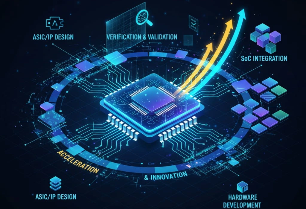
At OptM Solutions, we empower semiconductor companies to accelerate innovation across the complete silicon lifecycle — from ASIC design and verification to post-silicon validation. Our expertise spans IP design, SoC integration, and hardware development, helping clients achieve performance, scalability, and cost efficiency.
Core Capabilities
- IP Design
We specialize in developing high-performance IPs for high-speed interfaces, memory controllers, and mixed-signal applications, ensuring optimal performance and reliability.
- Test Chip Development
Our team delivers end-to-end test chip development for mixed-signal IPs, covering design, validation, and prototyping.
- SoC / Subsystem Integration
We offer proven expertise in integration, front-end tool flow setup, and functional analysis to ensure seamless subsystem interaction and design efficiency.
- IP Maintenance & Support
We provide long-term support for legacy IPs, including feature enhancements, post-silicon bug fixes, process migrations, and SoC integration assistance.
Our Specialized Expertise
ASIC / FPGA Capabilities
- New designs and die-size reduction
- Cost optimization and feature enhancement
- Silicon validation and performance tuning
Verification Services
- Module, block, and full-chip verification
- Protocol and testbench development
- Verification IP creation
- SoC, subsystem, and IP-level validation (C/SV/ASM-based)
Silicon Validation
- Test chip, reference board, and test board development
- Layout by IPC-certified engineers
- Prototyping and physical design solutions
IP Validation
- Bench characterization and testing
- Jitter profiling for IPs
- LDOs, BGRs, PORs, and temperature sensor validation
Hardware Design Services
- Development platforms and System-on-Modules (SoM)
- Embedded processor-based and power-optimized designs
- Small-footprint, rugged, and battery-operated solutions
- PCB layout, analysis, and multi-core/multi-processor hardware design
ASIC/FPGA Design & Verification Details
A look into our SystemVerilog RTL design, logic synthesis, and UVM validation workflows.
Frequently Asked Questions
Can your team assist with maintaining and upgrading our older, legacy IP blocks?
How do you handle the prototyping of extremely large ASIC designs?
What specific physical hardware and PCB design services do you offer?
Do you provide end-to-end support for mixed-signal test chips?
What specific validation frameworks are included in your chip design services?
Do your ic design services cover complex mixed-signal applications?
Why Us
Rapid Prototyping & FPGA Partitioning
Fast turn-around prototyping services that translate multi-million gate ASIC designs into scalable FPGA implementations.
Reusable & Scalable Verification
Development of reusable verification environments that accelerate IP/SoC validation and ensure quality across projects.
Test Chip Expertise
Proven end-to-end experience in mixed-signal IP test chip design, verification, and characterization.
Broad Semiconductor Services Portfolio
Comprehensive support across ASIC design, verification, physical design, layout, and FPGA development.
Related Services
Explore our other engineering and technology services.
.webp)
Embedded Systems
Full lifecycle embedded system engineering from hardware design to firmware development.

Android OS Services
Custom Android OS customization, HAL development, and BSP optimization for embedded devices.
.webp)
Model Based Design
MBD services using MATLAB/Simulink for controls, simulation, and auto-code generation.